
中文词条原文链接(无法从中国内地访问):请点击这里访问
英文词条原文链接(无法从中国内地访问):请点击这里访问
本文基于英文词条的线索,并补充部分来自中文词条的内容(在二者冲突时,以更晚更新者为准)。辽观搬运时进行了必要的合规化处理,以使其能够在中国内地上传。维基百科(Wikipedia)是美国维基媒体基金会的互联网百科项目,其内容可能受到立场、信息来源等因素影响,请客观看待。正文内容不代表译者观点。
辽观提供的翻译仅供参考。文中可能包含无法从中国内地访问的链接。
辽观所搬运的词条文本与维基百科一道同样遵循CC BY-SA 4.0协议(辽观搬运的中英文对照版本),在符合协议要求的情况下您可以免费使用其内容(包括商用)。图片和视频可能遵循不同的共享协议。请点击这里访问
注:全文在本站的词条均由于某些原因无法在知乎专栏发布,其中可能包含与您预设立场不同的内容。辽观出于提供参考资料的考量未对此作出处理,请您理性看待。
图片题注:这是一个企业、组织、政府或其他形式团体的标志,在台湾积体电路制造条目中使用。
图片作者:撷取自2022年度报告
A. 正文(全文在本站)
【维基百科的消歧义提示】Not to be confused with Taiwan Semiconductor Company Limited.
【参考译文】请注意,这里提到的是台湾积体电路制造股份有限公司(TSMC),与台湾半导体股份有限公司(TSMC)不要混淆。
0. 概述
辽观注:此标题是我们在搬运、整合过程中添加的。

图片题注:One of TSMC’s factories in Taichung’s Central Taiwan Science Park
图片作者:Briáxis F. Mendes (孟必思)
参考译文:台积电在台中中部台湾科学园区的工厂之一
0.1 文字说明
辽观注:此标题是我们在搬运、整合过程中添加的。
台湾积体电路制造公司(英语:Taiwan Semiconductor Manufacturing Company Limited),简称TSMC、台积电、台积或台积公司[3],与旗下公司合称时则称作台积电集团[4][5],为台湾一家从事晶圆代工的公司。总部位于台湾新竹科学园区。
2021年8月,台积电在美国《财富》杂志评选“全球最大500家公司”排行榜中,依营收规模名列全球第251名[6]。
Taiwan Semiconductor Manufacturing Company Limited (TSMC; also called Taiwan Semiconductor)[4][5] is a Taiwanese multinational semiconductor contract manufacturing and design company. It is the world’s second most valuable semiconductor company,[6] the world’s largest dedicated independent (“pure-play“) semiconductor foundry,[7] and its country’s largest company,[8][9] with headquarters and main operations located in the Hsinchu Science Park in Hsinchu, Taiwan. It is majority owned by foreign investors,[10] and the central government of Taiwan is the largest shareholder.[11] In 2023, the company was ranked 44th in the Forbes Global 2000.[12]
【参考译文】台湾积体电路制造股份有限公司(TSMC;也称为台湾积体)是一家台湾跨国半导体代工和设计公司。它是世界第二大市值的半导体公司,全球最大的独立(“纯粹代工”)半导体晶圆厂,以及台湾最大的公司,总部和主要业务位于台湾新竹科学园区。该公司大部分股权由外国投资者持有,台湾中央政府是最大的股东。到2023年,该公司在《福布斯全球2000强》排名第44位。
TSMC was founded in Taiwan in 1987 by Morris Chang as the world’s first dedicated semiconductor foundry. It has long been the leading company in its field.[13][14] When Chang retired in 2018, after 31 years of TSMC leadership, Mark Liu became chairman and C. C. Wei became Chief Executive.[15][16] It has been listed on the Taiwan Stock Exchange (TWSE: 2330) since 1993; in 1997 it became the first Taiwanese company to be listed on the New York Stock Exchange (NYSE: TSM). Since 1994, TSMC has had a compound annual growth rate (CAGR) of 17.4% in revenue and a CAGR of 16.1% in earnings.[17]
【参考译文】台积电成立于1987年,由张忠谋在台湾创立,是全球第一家专注于半导体代工的公司。长期以来一直是该领域的领先公司。张忠谋在担任台积电领导31年后于2018年退休,由刘德音担任董事长,魏哲家担任首席执行官。自1993年以来,台积电一直在台湾证券交易所上市(股票代码:2330);1997年,它成为首家在纽约证券交易所上市的台湾公司(股票代码:TSM)。自1994年以来,台积电的营收年复合增长率为17.4%,盈利年复合增长率为16.1%。
Most of the leading fabless semiconductor companies such as AMD, Apple, ARM, Broadcom, Marvell, MediaTek, Qualcomm and Nvidia, are customers of TSMC, as are emerging companies such as Allwinner Technology, HiSilicon, Spectra7, and UNISOC.[18] Leading programmable logic device companies Xilinx and previously Altera also make or made use of TSMC’s foundry services.[19] Some integrated device manufacturers that have their own fabrication facilities, such as Intel, NXP, STMicroelectronics and Texas Instruments, outsource some of their production to TSMC.[20][21] At least one semiconductor company, LSI, re-sells TSMC wafers through its ASIC design services and design IP portfolio.[dubious – discuss]
【参考译文】大多数领先的无晶圓厂半导体公司,如AMD、Apple、ARM、Broadcom、Marvell、联发科、高通和英伟达,都是台积电的客户,同时新兴公司如全志科技、海思、Spectra7和展讯也是其客户。领先的可编程逻辑器件公司赛灵思以及之前的Altera也使用或曾使用过台积电的代工服务。一些拥有自己制造设施的集成器件制造商,如英特尔、恩智浦、意法半导体和德州仪器,将部分生产外包给台积电。至少有一家半导体公司LSI通过其ASIC设计服务和设计IP组合重新销售台积电晶圆。
TSMC has a global capacity of about thirteen million 300 mm-equivalent wafers per year as of 2020 and makes chips for customers with process nodes from 2 microns to 3 nanometres. TSMC was the first foundry to market 7-nanometre and 5-nanometre (used by the 2020 Apple A14 and M1 SoCs, the MediaTek Dimensity 8100, and AMD Ryzen 7000 series processors) production capabilities, and the first to commercialize extreme ultraviolet (EUV) lithography technology in high volume.
【参考译文】截至2020年,台积电的全球产能约为每年1300万片300毫米等效晶圆,并为客户生产工艺节点从2微米到3纳米的芯片。台积电是第一个推出7纳米和5纳米生产能力的代工厂(2020年苹果A14和M1 SoC、联发科天玑8100和AMD锐龙7000系列处理器采用了5纳米工艺),也是第一个大规模商业化极紫外(EUV)光刻技术的代工厂。
0.2 概况表格
辽观注:此标题是我们在搬运、整合过程中添加的。
| 商业名称 | 台积电(TSMC) |
|---|---|
| 公司类型 | 上市公司 |
| 股票代号 | 台证所:2330 (1994年9月5日上市) NYSE:TSM (1997年10月20日上市) LSE:0LCV FWB:TSFA |
| ISIN | US8740391003 |
| 统一编号 | 22099131 |
| 成立 | 1987年2月21日 |
| 创办人 | 张忠谋 |
| 代表人物 | 董事长:刘德音 副董事长兼总裁:魏哲家 执行副总经理 暨共同首席运营官:米玉杰、秦永沛 |
| 总部 | 台湾 300096 新竹市东区力行六路8号 |
| 标语口号 | 诚信正直.承诺.创新.客户信任 |
| 业务范围 | |
| 产业 | 半导体 |
| 产品 | 晶圆代工服务 |
| 营业额 | revenue | |
| 息税前利润 | operating income | |
| 净利润 | net income | |
| 总资产 | total assets | |
| 资产净值 | total equity | |
| 员工人数 | |
| 实收资本额 | 新台币259,303,804,580元 |
| 市值 | ▲新台币14.29兆元(2023年8月10日) |
| 每股盈利 | ▲新台币23.01元(2021年) |
| 每股资产净值 | ▲新台币96.27元(2022年Q2) |
| 主要股东 | 美国花旗银行托管台积电存托证书专户(20.52%) 国发会(6.38%) |
| 主要子公司 | 30家[2] |
| 网站 | www.tsmc.com |
1. 历史
1.1 1970-2000年代
1974年时任中华民国经济部部长的孙运璿决定从美国引进集成电路制造工业,在工业技术研究院成立“电子工业研究发展中心”(今的电子所),负责集成电路工业研发,由经济部出资1000万美元的RCA技术移转计划。
In 1986, Li Kwoh-ting, representing the Executive Yuan, invited Morris Chang to serve as the president of the Industrial Technology Research Institute (ITRI) and offered him a blank check to build Taiwan’s chip industry. At that time, the Taiwanese government wanted to develop its semiconductor industry, but its high investment and high risk nature made it difficult to find investors. Texas Instruments and Intel turned down Chang. Only Philips was willing to sign a joint venture contract with Taiwan to put up $58 million, transfer its production technology, and license intellectual property in exchange for a 27.5 percent stake in TSMC. Alongside generous tax benefits, the Taiwanese government provided another 48 percent of the startup capital for TSMC, and the rest of the capital was raised from several of the island’s wealthiest families, who owned firms that specialized in plastics, textiles, and chemicals. These wealthy Taiwanese were directly “asked” by the government to invest. “What generally happened was that one of the ministers in the government would call a businessman in Taiwan,” Chang explained, “to get him to invest.” From day one, TSMC was not really a private business: it was a project of the Taiwanese state.[22][23][24] Its first CEO was James E. Dykes, who left after a year and Morris Chang became the CEO.[25]
【参考译文】1986年,代表行政院的李国鼎邀请张忠谋担任工业技术研究院(ITRI)的总裁,并提供一张空白支票来建立台湾的芯片产业。当时,台湾政府希望发展半导体产业,但其高投资和高风险性使其很难找到投资者。德州仪器和英特尔都拒绝了张忠谋。只有飞利浦愿意与台湾签署合资合同,提供5800万美元,转让其生产技术,并授权知识产权,以换取TSMC 27.5%的股份。除了慷慨的税收优惠外,台湾政府还提供TSMC成立时的另外48%的启动资本,其余资本则来自该岛上几个最富裕的家族,他们拥有专门从事塑料、纺织和化学产品的公司。这些富裕的台湾人是直接被政府“要求”投资的。张忠谋解释说:“通常情况下,政府的一位部长会打电话给台湾的一位商人,请他投资。”从一开始,TSMC并不是一家真正的私营企业:它是台湾政府的一个项目。它的第一任首席执行官是詹姆斯·E·戴克斯(James E. Dykes),他在一年后离开,张忠谋成为首席执行官。
1994年,台积电在台湾证券交易所挂牌上市。1997年,赴美国纽约证券交易所(NYSE)发行美国存托证书(ADR),并以TSM为代号开始挂牌交易。
1998年台积电文教基金会成立,期望透过致力于参与各项教育文化及社会公益活动来反馈社会。[7]
1.2 2000-2010年代
Since then, the company has continued to grow, albeit subject to the cycles of demand. In 2011, the company planned to increase research and development expenditures by almost 39% to NT$50 billion to fend off growing competition.[26] The company also planned to expand capacity by 30% in 2011 to meet strong market demand.[27] In May 2014, TSMC’s board of directors approved capital appropriations of US$568 million to increase and improve manufacturing capabilities after the company forecast higher than expected demand.[28] In August 2014, TSMC’s board of directors approved additional capital appropriations of US$3.05 billion.[29]
【参考译文】自那时起,台积电继续增长,尽管受到需求周期的影响。2011年,该公司计划将研发支出增加近39%,达到500亿元新台币,以应对不断增长的竞争压力。该公司还计划在2011年将产能扩大30%,以满足强劲的市场需求。2014年5月,台积电董事会批准拨款5.68亿美元,以增加和改进生产能力,因为公司预测需求高于预期。2014年8月,台积电董事会又批准额外拨款30.5亿美元。
In 2011, it was reported that TSMC had begun trial production of the A5 SoC and A6 SoCs for Apple’s iPad and iPhone devices.[30][31] According to reports,[32] in May 2014 Apple sourced its A8 and A8X SoCs from TSMC.[33][34] Apple then sourced the A9 SoC with both TSMC and Samsung (to increase volume for iPhone 6S launch) and the A9X exclusively with TSMC, thus resolving the issue of sourcing a chip in two different microarchitecture sizes. As of 2014, Apple was TSMC’s most important customer.[34][35]
【参考译文】2011年,有报道称台积电已开始为苹果的iPad和iPhone设备试生产A5 SoC和A6 SoC。据报道,2014年5月,苹果从台积电采购了A8和A8X SoC。之后,苹果为了增加iPhone 6S的产量,同时从台积电和三星采购了A9 SoC,而A9X则专门从台积电采购,从而解决了在两种不同微架构尺寸中寻找芯片的问题。截至2014年,苹果是台积电最重要的客户。
In October 2014, ARM and TSMC announced a new multi-year agreement for the development of ARM based 10 nm FinFET processors.[36]
【参考译文】2014年10月,ARM和台积电宣布了一项新的多年协议,用于开发基于ARM架构的10纳米FinFET处理器。
2015年年底,台积电月产能达189万片8英寸约当晶圆,是全球最大逻辑IC产能的半导体厂[8]。
赴中国(大陆)设厂
台积电在本地以外的第一站,是前往上海创办的十厂,以百分之百子公司的方式持有,新晶圆厂也位于上海,同时是该公司总部。2016年,台积电在中国的首座12英寸大型晶圆厂正式在南京市宣布动工[9],项目2018年投产[10]。2021年该厂再获投资,进入扩产阶段[11]。
市值超越IBM与英特尔
2016年9月19日,台积电市值首度超越美国电子巨擘IBM[12]。2017年3月20日,台积电市值首度超越美国芯片巨擘英特尔[13]。9月29日,台积电宣布未来3纳米工艺晶圆厂,落脚台湾南部科学园区,预计最快2022年量产[14]。10月2日,时任董事长张忠谋宣布将于2018年6月份卸任董事长和总裁,届时将由刘德音接任董事长、魏哲家接任台积电总裁。[15]
1.3 2020年代
1.3.1 中美贸易战和欧美建厂
辽观注:此标题是我们在搬运、整合过程中添加的。
主条目:中美贸易战
2019年美国商务部宣布新规定,凡使用美国半导体技术与设备的外国企业,必须先获取许可,将中国大陆网通设备巨头厂商华为及旗下数百家子公司纳入出口管制黑名单,禁止华为在没有政府当局核准的情况下,向任何使用美国技术的企业购买零组件。而当时市场研判是针对台积电,当时台积电的客户群中有百分之十五是华为。
2020年,台积电开始往欧洲与美国建造新工厂集,将赴美国亚利桑那州设厂,投入1000亿元[16]。创办人张忠谋在4月份的一次演讲中回应,强调台积电的成功与台湾人密不可分,更需要保住和重视台积电[17]。2023年7月,位于新竹县宝山乡的台积电全球研发中心激活。
赴德国设厂制造
2023年8月8日,台积电与罗伯特博世公司(Robert Bosch GmbH)、英飞凌科技股份公司(Infineon Technologies AG)和恩智浦半导体( NXP Semiconductors N.V.)合作投资“欧洲集成电路制造”(European Semiconductor Manufacturing Company,ESMC)品牌[18],生产先进汽车芯片,规模依据欧洲芯片法案(European Chips Act)审核为定[19],于德国德累斯顿设置设置晶圆厂进行制造[20]。
赴美国设直营厂
2020年5月14日,台积电宣布将在美国设立新厂,确定斥资120亿美元,设立5纳米工艺的晶圆厂,场址在亚利桑那州菲尼克斯。台积电亚利桑那州厂占地约445公顷,工程总投资金额约400亿美元,为美国史上规模最大的外国直接投资案之一。于2021年4月动工,2022年12月6日举行首批机台设备到厂典礼,2025年开始量产[21]
赴日本设厂
2021年10月14日,台积电获得在日本九州之开设晶圆代工厂的项目,宣布该厂为全新的子公司“日本先进半导体制造”(Japan Advanced Semiconductor Manufacturing,JASM),合资的JASM会为台积公司在日本当地生产之的代工服务部门,以22纳米至28纳米的工艺为主,2022年熊本 (一)厂开工[22]、2024年2月完工激活;2024年2月再宣布将建熊本二厂[23]。
1.3.2 企业经营情况
辽观注:此标题是我们在搬运、整合过程中添加的。
In 2020, TSMC became the first semiconductor company in the world to sign up for the RE100 initiative, pledging to use 100% renewable energy by 2050.[37] TSMC accounts for roughly 5% of the energy consumption in Taiwan, even exceeding that of the capital city Taipei. This initiative was thus expected to accelerate the transformation to renewable energy in the country.[38]
【参考译文】在2020年,台积电成为全球第一家签署RE100倡议的半导体公司,承诺到2050年实现100%使用可再生能源。台积电约占据台湾能源消耗的5%,甚至超过台湾首都台北市的能源消耗。因此,这一倡议预计将加速台湾向可再生能源转型的进程。
For 2020, TSMC had a net income of US$17.60 billion on a consolidated revenue of US$45.51 billion, an increase of 57.5% and 31.4% respectively from the 2019 level of US$11.18 billion net income and US$34.63 billion consolidated revenue.[39] Its market capitalization was over $550 billion[clarification needed] in April 2021.[citation needed] TSMC’s revenue in the first quarter of 2020 reached US$10 billion,[40] while its market capitalization was US$254 billion.[41] TSMC’s market capitalization reached a value of NT$1.9 trillion (US$63.4 billion) in December 2010.[42] It was ranked 70th in the FT Global 500 2013 list of the world’s most highly valued companies with a capitalization of US$86.7 billion,[43] while reaching US$110 billion in May 2014.[41] In March 2017, TSMC’s market capitalization surpassed that of semiconductor giant Intel for the first time, hitting NT$5.14 trillion (US$168.4 billion), with Intel’s at US$165.7 billion.[44] On 27 June 2020, TSMC briefly became the world’s 10th most valuable company, with a market capitalization of US$410 billion.[45]
【参考译文】截至2020年,台积电的净利润为176亿美元,合并营收为455.1亿美元,分别比2019年的净利润111.8亿美元和合并营收346.3亿美元增长了57.5%和31.4%。2021年4月,台积电的市值超过5500亿美元。2020年第一季度,台积电的营收达到了100亿美元,市值为2540亿美元。2010年12月,台积电的市值达到了1.9万亿新台币(634亿美元)。2013年,台积电在FT全球500强中排名第70位,市值为867亿美元;2014年5月,市值增至1,100亿美元。2017年3月,台积电的市值首次超过半导体巨头英特尔,达到了5.14万亿新台币(1684亿美元),而英特尔的市值为1657亿美元。2020年6月27日,台积电短暂成为全球第十大市值公司,市值达到了4100亿美元。
In June 2021, following nearly a year of public controversy surrounding its COVID-19 vaccine shortage,[51][52][53][54] with only about 10% of its 23.5 million population vaccinated;[51] Taiwan agreed to allow TSMC and Foxconn to jointly negotiate purchasing COVID-19 vaccines on its behalf.[53][51] In July 2021, BioNTech‘s Chinese sales agent Fosun Pharma announced that the two technology manufacturers had reached an agreement to purchase 10 million BioNTech COVID-19 vaccines from Germany.[53][51] TSMC and Foxconn pledged to each buy five million doses for up to $175 million,[53] for donation to Taiwan’s vaccination program.[51]
【参考译文】2021年6月,经历了近一年的关于COVID-19疫苗短缺的公开争议,台湾仅有大约2350万人口中的约10%接种了疫苗。台湾同意让台积电和富士康代表其共同协商购买COVID-19疫苗。2021年7月,BioNTech的中国销售代理复宏智汇宣布,这两家科技制造商已达成协议,从德国购买1000万剂BioNTech COVID-19疫苗。台积电和富士康承诺分别购买500万剂,总计最高1750万美元,捐赠给台湾的疫苗接种计划。
Due to the 2020–2023 global semiconductor shortage, Taiwanese competitor United Microelectronics raised prices approximately 7–9 percent, and prices for TSMC’s more mature processors will be raised by about 20 percent.[55]
【参考译文】由于2020年至2023年全球半导体短缺的影响,台湾竞争对手联电将价格提高了约7-9%,而台积电更成熟处理器的价格将提高约20%。
In November 2021, TSMC and Sony announced that TSMC would be establishing a new subsidiary named Japan Advanced Semiconductor Manufacturing [ja; zh] (JASM) in Kumamoto, Japan. The new subsidiary will manufacture 22- and 28-nanometer processes. The initial investment will be approximately $7 billion, with Sony investing approximately $500 million for a less than 20% stake. Construction of the fabrication plant is expected to start in 2022, with production targeted to begin two years later in 2024.[56][57]
【参考译文】2021年11月,台积电和索尼宣布,台积电将在日本熊本设立一个名为日本先进半导体制造(JASM)的新子公司。这家新子公司将生产22纳米和28纳米工艺。初始投资约为70亿美元,索尼将投资约5亿美元,持有不到20%的股份。该生产厂的建设预计将于2022年开始,生产计划于2024年开始。
In February 2022, TSMC, Sony Semiconductor Solutions, and Denso announced that Denso would take a more than 10% equity stake in JASM with a US$0.35 billion investment, amid a scarcity of chips for automobiles.[58][59][60] TSMC will also enhance JASM’s capabilities with 12/16 nanometer FinFET process technology in addition to the previously announced 22/28 nanometer process and increase monthly production capacity from 45,000 to 55,000 12-inch wafers.[58][59][60] The total capital expenditure for JASM’s Kumamoto fab is estimated to be approximately US$8.6 billion.[58][59][60] The Japanese government wants JASM to supply essential chips to Japan’s electronic device makers and auto companies as trade friction between the United States and China threatens to disrupt supply chains.[58][59][60] The fab is expected to directly create about 1,700 high-tech professional jobs.[58][59]
【参考译文】在2022年2月,台积电、索尼半导体解决方案和电装宣布,鉴于汽车芯片短缺的情况,电装将通过投资3.5亿美元,持有超过10%的JASM股权。除了之前宣布的22/28纳米工艺,台积电还将利用12/16纳米FinFET工艺技术增强JASM的能力,并将月生产能力从45,000片12英寸晶圆增加到55,000片。JASM熊本工厂的总资本支出预计约为86亿美元。日本政府希望JASM向日本的电子设备制造商和汽车公司提供必要的芯片,因为美国和中国之间的贸易摩擦有可能扰乱供应链。预计该工厂将直接创造约1700个高科技专业岗位。
In July 2022, TSMC announced the company had posted a record profit in the second quarter, with net income up 76.4 percent year-over-year. The company saw steady growth in the automotive and data center sectors with some weakness in the consumer market. Some of the capital expenditures are projected to be pushed up to 2023.[61]
【参考译文】2022年7月,台积电宣布公司第二季度实现了创纪录的利润,净利润同比增长76.4%。该公司在汽车和数据中心领域实现稳定增长,但在消费市场方面存在一些疲软。预计部分资本支出将推迟至2023年。
In the third quarter of 2022, Berkshire Hathaway disclosed purchase of 60 million shares in TSMC, acquiring a $4.1 billion stake, making it one of its largest holdings in a technology company.[62] However, Berkshire sold off 86.2% of its stake by the next quarter citing geopolitical tensions as a factor.[63][64]
【参考译文】在2022年第三季度,伯克希尔-哈撒韦公司披露购买了台积电6000万股,获得了价值41亿美元的股份,成为其在科技公司中的最大持股之一。然而,到了下一个季度,伯克希尔出售了其86.2%的股份,称地缘政治紧张局势是一个因素。
In February 2024, TSMC shares hit a record high, with the high on the trading day reaching NT$709 and closing at NT$697 (+8%). This was influenced by the increase in the price target on chip designer Nvidia. TSMC currently manufactures 3-nanometer chips and plans to start 2-nanometer mass production in 2025.[65]
【参考译文】在2024年2月,台积电股价创下历史新高,交易日的最高价达到新台币709元,并以新台币697元(上涨8%)收盘。这一涨势受到芯片设计公司英伟达(Nvidia)价格目标上调的影响。台积电目前生产3纳米芯片,并计划在2025年开始2纳米芯片的量产。
1.3.3 与格罗方德的专利纠纷 | Patent dispute with GlobalFoundries
On 26 August 2019, GlobalFoundries filed several patent infringement lawsuits against TSMC in the US and Germany claiming that TSMC’s 7 nm, 10 nm, 12 nm, 16 nm, and 28 nm nodes infringed 16 of their patents.[66] GlobalFoundries named twenty defendants.[67] TSMC said that they were confident that the allegations were baseless.[68]
【参考译文】2019年8月26日,GlobalFoundries在美国和德国对台积电提起了多项专利侵权诉讼,声称台积电的7纳米、10纳米、12纳米、16纳米和28纳米工艺侵犯了他们的16项专利。GlobalFoundries列举了二十名被告。台积电表示他们对这些指控毫无根据感到自信。
On 1 October 2019, TSMC filed patent infringement lawsuits against GlobalFoundries in the US, Germany and Singapore, claiming that GlobalFoundries’ 12 nm, 14 nm, 22 nm, 28 nm and 40 nm nodes infringed 25 of their patents.[69]
【参考译文】2019年10月1日,台积电在美国、德国和新加坡对GlobalFoundries提起了专利侵权诉讼,声称GlobalFoundries的12纳米、14纳米、22纳米、28纳米和40纳米工艺侵犯了他们的25项专利。
On 29 October 2019, TSMC and GlobalFoundries announced a resolution to the dispute, agreeing to a life-of-patents cross-license for all of their existing semiconductor patents and new patents for the next 10 years.[70][71][72][73][74]
【参考译文】2019年10月29日,台积电和GlobalFoundries宣布解决了纠纷,同意在所有现有半导体专利和未来10年内的新专利上进行终身专利交叉许可。
1.3.4 销量和市场趋势 | Sales and market trends
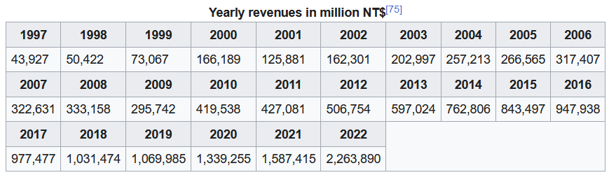
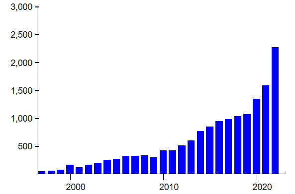
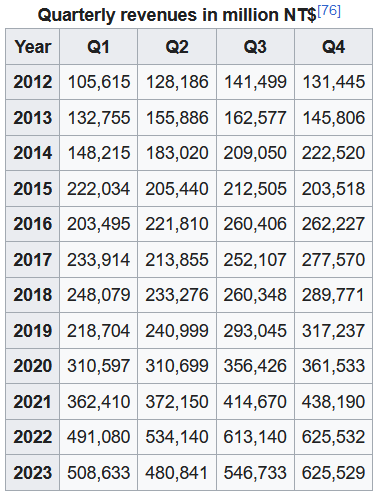
TSMC and the rest of the foundry industry are exposed to the cyclical industrial dynamics of the semiconductor industry. TSMC must ensure its production capacity to meet strong customer demand during upturns. However, during downturns, it must contend with excess capacity because of weak demand and the high fixed costs associated with its manufacturing facilities.[77] As a result, the company’s financial results tend to fluctuate with a cycle time of a few years. This is more apparent in earnings than revenues because of the general trend of revenue and capacity growth. TSMC’s business has generally also been seasonal, with a peak in Q3 and a low in Q1.
【参考译文】台积电和整个晶圆代工行业都受制于半导体行业的周期性工业动态。在行业景气时,台积电必须确保其生产能力以满足强劲的客户需求。然而,在行业低迷时,由于需求疲弱和其制造设施相关的高固定成本,公司必须应对产能过剩的问题。因此,公司的财务业绩往往会随着几年周期而波动。这种波动在收益方面比在营收方面更为明显,这是因为总体趋势是收入和产能增长。台积电的业务通常也呈季节性变化,第三季度是销售高峰,而第一季度是销售低谷。
In 2014, TSMC was at the forefront of the foundry industry for high-performance, low-power applications,[78][79] leading major smartphone chip companies such as Qualcomm,[80][81] Mediatek[81][82] and Apple[33][35] to place an increasing amount of orders.[78] While the competitors in the foundry industry (primarily GlobalFoundries and United Microelectronics Corporation) have encountered difficulties ramping leading-edge 28 nm capacity,[82] the leading Integrated Device Manufacturers such as Samsung and Intel that seek to offer foundry capacity to third parties were also unable to match the requirements for advanced mobile applications.[79]
【参考译文】2014年,台积电在高性能、低功耗应用领域处于晶圆代工行业的前沿,领先于高通、联发科和苹果等主要智能手机芯片公司,这些公司纷纷增加了在台积电的订单量。与晶圆代工行业的竞争对手(主要是GlobalFoundries和联电)遇到困难难以推广领先的28纳米产能不同,寻求向第三方提供代工能力的领先综合器件制造商,如三星和英特尔,也无法满足先进移动应用的要求。
For most of 2014, TSMC saw a continuing increase in revenues due to increased demand, primarily due to chips for smartphone applications. TSMC raised its financial guidance in March 2014 and posted ‘unseasonably strong’ first-quarter results.[28][83] For Q2 2014, revenues came in at NT$183 billion, with 28 nm technology business growing more than 30% from the previous quarter.[84] Lead times for chip orders at TSMC increased due to a tight capacity situation, putting fabless chip companies at risk of not meeting their sales expectations or shipment schedules,[85] and in August 2014 it was reported that TSMC’s production capacity for the fourth quarter of 2014 was already almost fully booked, a scenario that had not occurred for many years, which was described as being due to a ripple-effect due to TSMC landing CPU orders from Apple.[86]
【参考译文】在2014年的大部分时间里,由于需求增加,主要是智能手机应用芯片的需求增加,台积电的收入持续增长。台积电在2014年3月提高了自己的财务指引,并发布了“异常强劲”的第一季度业绩。2014年第二季度,台积电的营收达到了新台币1,830亿元,28纳米技术业务较上一季度增长超过30%。由于产能紧张,导致芯片订单的交货时间延长,使得无晶圆厂的芯片公司面临无法满足销售预期或发货计划的风险。2014年8月,报道称,台积电在2014年第四季度的生产能力几乎已经完全预订,这种情况多年来尚未发生过,这被描述为由于台积电获得了苹果的CPU订单而产生的连锁反应效应。
However, monthly sales for 2014 peaked in October, decreasing by 10% in November due to cautious inventory adjustment actions taken by some of its customers.[87] TSMC’s revenue for 2014 saw growth of 28% over the previous year, while TSMC forecasted that revenue for 2015 would grow by 15 to 20 percent from 2014, thanks to strong demand for its 20 nm process, new 16 nm FinFET process technology as well as continuing demand for 28 nm, and demand for less advanced chip fabrication in its 200mm fabs.[87]
【参考译文】然而,2014年的每月销售额在10月份达到峰值,但由于一些客户谨慎的库存调整行动,11月份下降了10%。台积电2014年的营收同比增长了28%,而台积电预测2015年的营收将比2014年增长15%至20%,这要归功于对其20纳米工艺、新的16纳米FinFET工艺技术以及持续对28纳米的需求,以及对其200毫米晶圆厂 less advanced芯片制造的需求。
2. 技术 | Technologies
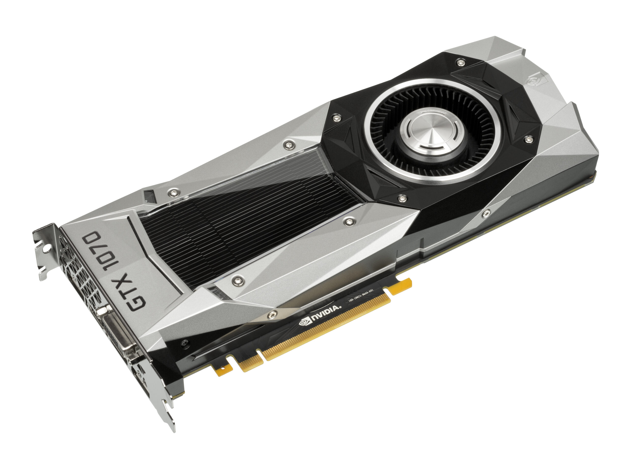
图片题注:The NVIDIA GeForce GTX 1070, which uses the GP104 die manufactured by TSMC on its 16 nm node
参考译文:NVIDIA GeForce GTX 1070使用了TSMC在其16纳米工艺节点上制造的GP104芯片。
图片作者:Evan-Amos
TSMC’s N7+ is the first commercially available extreme-ultraviolet lithographic process in the semiconductor industry.[88] It uses ultraviolet patterning and enables more acute circuits to be implemented on the silicon. N7+ offers a 15–20% higher transistor density and 10% reduction in power consumption than previous technology.[89][90] The N7 achieved the fastest ever volume time to market, faster than 10 nm and 16 nm.[91]
【参考译文】台积电的N7+是半导体行业中第一个商用的极紫外光刻工艺。它使用紫外光图案形成技术,能够在硅片上实现更精细的电路。N7+提供了比之前技术更高15-20%的晶体管密度,以及10%的功耗降低。N7实现了有史以来最快的量产市场时间,比10纳米和16纳米更快。
The N5 iteration doubles transistor density and improves performance by an additional 15%.[92][93]
【参考译文】N5版本将晶体管密度提高一倍,并将性能提升额外15%。
3. 营运及生产相关设施
台积电透过遍及全球的营运据点服务全世界半导体市场。全球总部位于新竹科学园区晶圆十二 A 厂。
3.1 工厂列表
辽观注:此标题是我们在搬运、整合过程中添加的。
晶圆厂区:
- 6 英寸晶圆厂
- 8 英寸晶圆厂
- 12 英寸晶圆厂[24]
先进封装测试厂
- 封测一厂: 竹科竹科园区
- 封测二厂: 南科台南园区
- 封测五厂: 中科台中园区
- 封测六厂: 竹科竹南园区
- 封测七厂: 南科嘉义园区(预计2024年5月动工,2026年完工,2028年量产)
- 封测八厂: 南科嘉义园区(预计2024年5月动工,2026年完工)
研发中心
员工学习中心
再生水厂
3.2 亚利桑那工厂 | Arizona
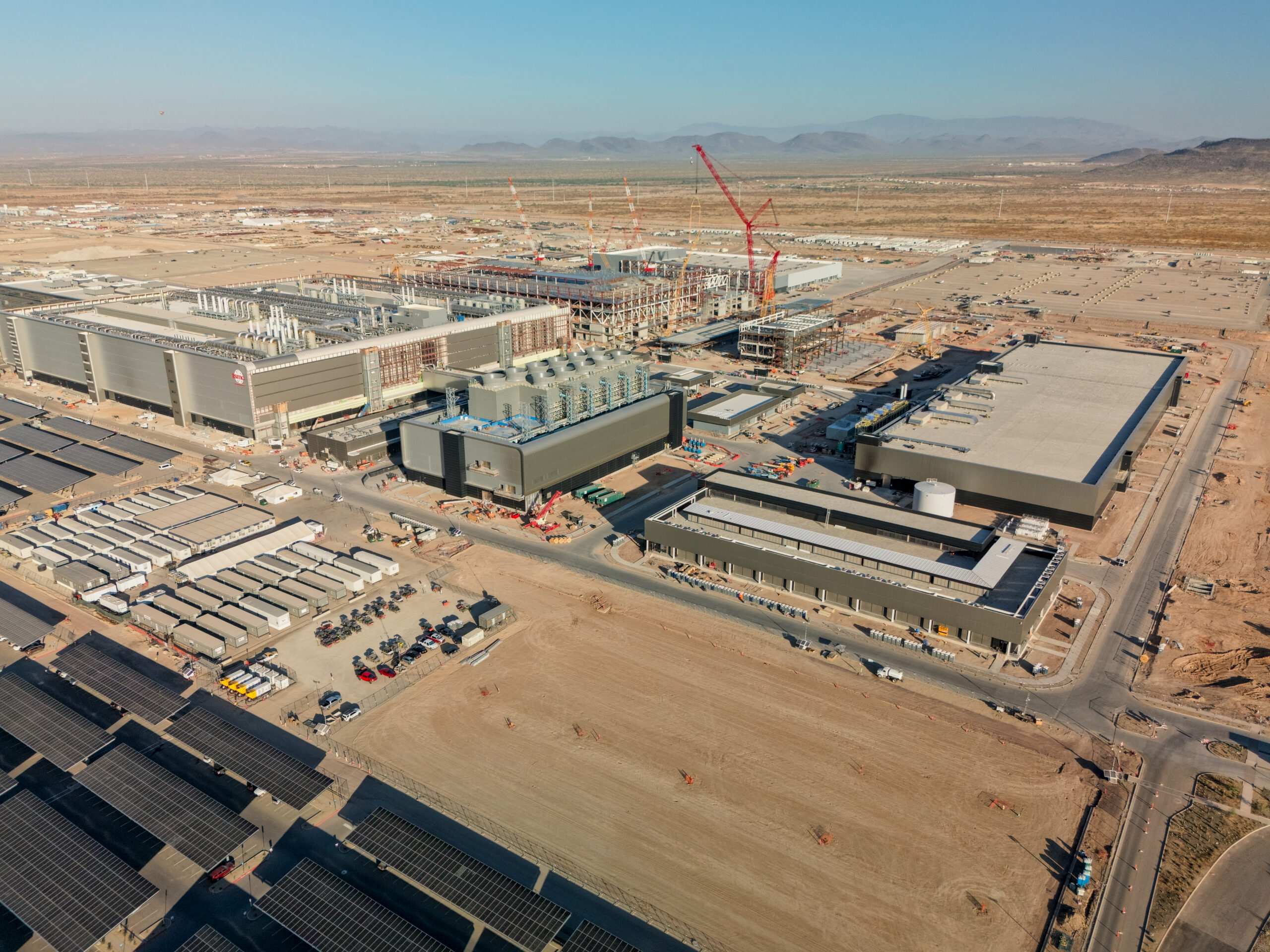
图片题注:Fab 21 under construction in Phoenix, Arizona in November 2023
参考译文:2023年11月,位于亚利桑那州凤凰城的Fab 21正在建设中。
图片作者:TrickHunter
In 2020, TSMC announced a planned fab in Phoenix, Arizona, intended to begin production by 2024 at a rate of 20,000 wafers per month. As of 2020, TSMC announced that it would bring its newest 5 nm process to the Arizona facility, a significant break from its prior practice of limiting US fabs to older technologies. The Arizona plant was estimated to not be fully operational until 2024, when the 5 nm process is projected to be replaced by TSMC’s 3 nm process as the latest technology.[108] At launch it will be the most advanced fab in the United States.[109] TSMC plans to spend $12 billion on the project over eight years, beginning in 2021.[108] TSMC claimed the plant will create 1,900 full-time jobs.[110]
【参考译文】2020年,台积电宣布计划在亚利桑那州凤凰城建设一座工厂,预计于2024年开始生产,产能为每月2万片晶圆。截至2020年,台积电宣布将在亚利桑那工厂引入最新的5纳米工艺,这与其之前将美国工厂限制在较老技术的做法有了显著的突破。预计亚利桑那工厂将在2024年前完全投产,届时5纳米工艺将被台积电的3纳米工艺取代成为最新技术。该工厂在投产时将成为美国最先进的工厂。台积电计划在2021年开始的八年时间里在该项目上投资120亿美元。台积电声称该工厂将创造1900个全职工作岗位。
In December 2022, TSMC announced its plans to triple its investment in the Arizona plants in response to the growing tensions between the US and China and the supply chain disruption that has led to chip shortages.[111] In that same month, TSMC stated that they were running into major cost issues, because the cost of construction of buildings and facilities in the US is four to five times what an identical plant would cost in Taiwan, (due to higher costs of labor, red tape, and training), as well as difficulty finding qualified personnel (for which it has hired US workers and sent them for training in Taiwan for 12–18 months.) These additional production costs will increase the cost of TSMC’s chips made in the US to at least 50% more than the cost of chips made in Taiwan.[112][113][114] In July 2023 TSMC warned that US talent was insufficient, so Taiwanese workers will need to be brought in for a limited time, and that the chip factory won’t be operational until 2025.[115] In September 2023, an analyst said the chips will still need to be sent back to Taiwan for packaging.[116] In January 2024, TSMC chairman Liu again warned that Arizona lacked workers with the specialized skills to hire and that TSMC’s second Arizona plant likely won’t start volume production of advanced chips until 2027 or 2028.[117]
【参考译文】2022年12月,台积电宣布计划将其在亚利桑那工厂的投资额增加三倍,以应对美中之间不断升级的紧张局势以及导致芯片短缺的供应链中断。同月,台积电表示他们遇到了主要的成本问题,因为在美国建设建筑和设施的成本是台湾的4到5倍(由于劳动力成本、繁文缛节和培训成本更高),同时也难以找到合格的人员(为此,公司已经聘用了美国员工并派他们到台湾接受12-18个月的培训)。这些额外的生产成本将使台积电在美国生产的芯片成本至少比在台湾生产的芯片成本高出50%。2023年7月,台积电警告称美国的人才不足,因此台湾工人将需要被引进一段有限的时间,并且芯片工厂直到2025年才能投入运营。2023年9月,一位分析师表示芯片仍需要被送回台湾进行封装。2024年1月,台积电董事长刘又警告称亚利桑那缺乏拥有专业技能的工人,台积电第二座亚利桑那工厂可能要等到2027年或2028年才会开始大规模生产先进芯片。
3.2 台中科学园 | Central Taiwan Science Park
The investment of US$9.4 billion to build its third 300mm wafer fabrication facility in Central Taiwan Science Park (Fab 15) was originally announced in 2010.[118] The facility was expected to manufacture over 100,000 wafers a month and generate US$5 billion per year of revenue.[119] TSMC has continued to expand advanced 28 nm manufacturing capacity at Fab 15.[120]
【参考译文】2010年,台积电宣布投资94亿美元在中台湾科学园区(Fab 15)建设第三座300毫米晶圆制造设施。这座工厂预计每月生产超过10万片晶圆,并产生每年50亿美元的收入。台积电继续在Fab 15扩大先进的28纳米制造能力。
On 12 January 2011, TSMC announced the acquisition of land from Powerchip Semiconductor for NT$2.9 billion (US$96 million) to build two additional 300mm fabs (Fab 12B) to cope with increasing global demand.[121]
【参考译文】2011年1月12日,台积电宣布从力晶半导体以29亿新台币(9600万美元)的价格收购土地,用于建设两座额外的300毫米晶圆厂(Fab 12B),以满足不断增长的全球需求。
3.3 WaferTech子公司 | WaferTech subsidiary
WaferTech, a subsidiary of TSMC, is a pure-play semiconductor foundry based in Camas, Washington, 32 km (20 mi) outside Portland, Oregon. The WaferTech campus contains a 9.3 ha (23 acres) complex housed on 105 ha (260 acres), with a main fabrication facility consisting of a 12,000 m2 (130,000 sq ft) 200mm wafer fabrication plant.[122] The site is the second-largest pure-play foundry in the United States, employing 1,100 workers.[citation needed] The largest is GlobalFoundries Fab 8 in Malta, New York, which employs over 3,000 workers with over 278,709 m2 (3,000,000 sq ft) under one roof.
【参考译文】WaferTech是台积电的子公司,是一家位于华盛顿州卡马斯市(距离俄勒冈州波特兰市外32公里,即20英里)的纯晶圆代工厂。WaferTech园区占地105公顷(260英亩),内含一个占地9.3公顷(23英亩)的综合大楼群,主要的制造设施包括一个面积为12,000平方米(130,000平方英尺)的200毫米晶圆制造厂。该工厂是美国第二大纯晶圆代工厂,员工数量为1,100人。全美最大的纯晶圆代工厂是全球闪存的Fab 8,在纽约州马尔他市,员工超过3,000人,占地面积超过278,709平方米(3,000,000平方英尺)。
As of 2024, the facility supports node sizes of 0.35, 0.30, 0.25, 0.22, 0.18, and 0.16 micrometers, with an emphasis on embedded flash process technology.[123]
【参考译文】截至2024年,该设施支持0.35、0.30、0.25、0.22、0.18和0.16微米等节点尺寸,重点放在嵌入式闪存工艺技术上。
3.3.1 历史 | History
WaferTech was established in June 1996 as a joint venture with TSMC, Altera, Analog Devices, and ISSI as key partners. The four companies and minor individual investors placed US$1.2 billion into this venture, which was at the time the single largest startup investment in the state of Washington. The company started production in July 1998 in its 200mm semiconductor fabrication plant. Its first product was a 0.35 micrometer part for Altera.[citation needed]
【参考译文】WaferTech成立于1996年6月,是与TSMC、Altera、Analog Devices和ISSI等重要合作伙伴共同成立的合资企业。这四家公司和少量个人投资者共同投资了12亿美元到这个合资项目中,当时这是华盛顿州单个最大的初创投资。该公司于1998年7月开始在其200mm半导体制造厂进行生产。其第一个产品是为Altera生产的0.35微米零部件。
TSMC bought out the joint venture partners in 2000 and acquired full control, operating it as a fully owned subsidiary.[124]
【参考译文】台积电于2000年收购了合资企业的合作伙伴,获得了全面控制权,并将其作为全资子公司运营。
In 2015, Dr. Tsung Kuo was named company president and fab director of WaferTech.[125]
【参考译文】2015年,曾冠博士被任命为WaferTech的公司总裁兼工厂总监。
3.4 德国 | Germany
In August 2023, TSMC committed 3.5 billion Euros to a 10+ billion Euro factory in Dresden, Germany, with participation of Robert Bosch GmbH, Infineon Technologies and NXP Semiconductors and a 5 billion Euro subsidy from the German government, in exchange for a 70% majority in the resulting European Semiconductor Manufacturing Company (ESMC).[126][127][128][129]
【参考译文】2023年8月,台积电承诺向德国德累斯顿投资35亿欧元,用于建设一座价值超过100亿欧元的工厂,参与合作的公司包括博世集团、英飞凌科技和恩智浦半导体,同时德国政府还提供了50亿欧元的补贴,作为换取在新成立的欧洲半导体制造公司(ESMC)中持有70%的控股权。
4. 产能 | Production capabilities
On 300 mm wafers, TSMC has silicon lithography on node sizes:
【参考译文】在300毫米晶圆上,台积电的硅片光刻工艺的节点尺寸有:
- 0.13 μm (options: general-purpose (G), low-power (LP), high-performance low-voltage (LV)).
【参考译文】0.13 μm(选项:通用(G),低功耗(LP),高性能低电压(LV))。 - 90 nm (based upon 80GC from Q4/2006),
【参考译文】90纳米(基于2006年第四季度的80GC)。 - 65 nm (options: general-purpose (GP), low-power (LP), ultra-low power (ULP), LPG).
【参考译文】65纳米(选项:通用(GP),低功耗(LP),超低功耗(ULP),LPG)。 - 55 nm (options: general-purpose (GP), low-power (LP)).
【参考译文】55纳米(选项:通用(GP),低功耗(LP))。 - 40 nm (options: general-purpose (GP), low-power (LP), ultra-low power (ULP)).[94]
【参考译文】40纳米(选项:通用(GP),低功耗(LP),超低功耗(ULP))。 - 28 nm (options: high-performance (HP), high-performance mobile (HPM), high-performance computing (HPC), high-performance low-power (HPL), low-power (LP), high-performance computing Plus (HPC+), ultra-low power (ULP)) with HKMG.[95]
【参考译文】28纳米(选项:高性能(HP),高性能移动(HPM),高性能计算(HPC),高性能低功耗(HPL),低功耗(LP),高性能计算加强版(HPC+),超低功耗(ULP)),采用HKMG工艺。 - 22 nm (options: ultra-low power (ULP), ultra-low leakage (ULL))[96]
【参考译文】22纳米(选项:超低功耗(ULP),超低漏电(ULL)。 - 20 nm[97]
- 16 nm (options: FinFET (FF), FinFET Plus (FF+), FinFET Compact (FFC))[98]
【参考译文】16纳米(选项:FinFET(FF),FinFET Plus(FF+),FinFET Compact(FFC))。 - 12 nm (options: FinFET Compact (FFC), FinFET Nvidia (FFN)), enhanced version of 16 nm process.[99]
【参考译文】12纳米(选项:FinFET Compact(FFC),FinFET Nvidia(FFN)),是16纳米工艺的增强版本。 - 10 nm (options: FinFET (FF))[100]
【参考译文】10纳米(选项:FinFET(FF))。 - 7 nm (options: FinFET (FF), FinFET Plus (FF+), FinFET Pro (FFP), high-performance computing (HPC))[101]
【参考译文】7纳米(选项:FinFET(FF),FinFET Plus(FF+),FinFET Pro(FFP),高性能计算(HPC))。 - 6 nm (options: FinFET (FF)), risk production started in Q1 2020, enhanced version of 7 nm process.[102]
【参考译文】6纳米(选项:FinFET(FF)),风险生产于2020年第一季度,是7纳米工艺的增强版本。 - 5 nm (options: FinFET (FF)).
【参考译文】5纳米(选项:FinFET(FF))。 - 4 nm (options: FinFET (FF)). risk production started in 2021, enhanced version of 5 nm process.【参考译文】4纳米(选项:FinFET(FF)),风险生产于2021年,是5纳米工艺的增强版本。
- 3 nm (options: FinFET (FF)). volume production started in Q4 2022[103]
【参考译文】3纳米(选项:FinFET(FF)),量产于2022年第四季度。
It also offers “design for manufacturing” (DFM) customer services.[104]
【参考译文】它还提供“制造设计”(DFM)客户服务。
In press publications, these processes will often be referenced, for example, for the mobile variant, simply by 7nmFinFET or even more briefly by 7FF.
【参考译文】在新闻出版物中,这些工艺通常会以简化形式引用,例如移动端变种可能会简称为7纳米FinFET,甚至更简短地称为7FF。
At the beginning of 2019, TSMC was advertising N7+, N7, and N6 as its leading edge technologies,[102]
【参考译文】在2019年初,台积电将N7+、N7和N6作为其领先技术进行推广。
As of June 2020, TSMC is the manufacturer selected for production of Apple‘s 5 nanometer ARM processors, as “the company plans to eventually transition the entire Mac lineup to its Arm-based processors, including the priciest desktop computers”.[105]
【参考译文】截至2020年6月,台积电被选中生产苹果的5纳米ARM处理器,因为“苹果计划最终将整个Mac系列转换为基于Arm架构的处理器,包括价格最高的台式电脑”。
In July 2020, TSMC signed a 20-year deal with Ørsted to buy the entire production of two offshore wind farms under development off Taiwan’s west coast. At the time of its signing, it was the world’s largest corporate green energy order ever made.[106]
【参考译文】在2020年7月,台积电与Ørsted签署了一项为期20年的协议,购买正在开发中的台湾西海岸两座海上风电场的全部产量。在签署时,这是有史以来全球最大的企业绿色能源订单。
In July 2021, both Apple and Intel were reported to be testing their proprietary chip designs with TSMC’s 3 nm production.[107]
【参考译文】2021年7月,据报道,苹果和英特尔都在测试他们自家芯片设计,使用台积电的3纳米制程生产。
5. 股权与市值
5.1 股权 | Ownership
截至2020年12月,台积电为台湾证券交易所发行量加权股价指数最大成份股。根据台积电公布的2020年度报告 20-F 文件,该公司最大股东为行政院国家发展基金管理会,持股比例 6.38%[33]。20-F 文件注明该公司在美国花旗银行开设托管台积电存托证书专户,并有 5,321,575,398 股普通股(占 21.8%)在该账户中。该存托证书专户仅为股票交易使用,并非美国花旗银行通过该账户持有台积电股份,并且非中华民国人士想要持有台积电的股份必须通过中华民国保管人(custodians)代持[33]。
Around 56% of TSMC shares are held by the general public and around 38% are held by institutions. The largest shareholders in early 2024 were:[130]
【参考译文】到2024年初,台积电大约56%的股份由普通公众持有,大约38%的股份由机构持有。2024年初,持有最多股份的股东包括:
- National Development Fund, Executive Yuan (6.38%)
- BlackRock (5.09%)
- Capital Research and Management Company (3.61%)
- Government of Singapore Investment Corporation (3.32%)
- Norges Bank (1.59%)
- Fidelity Investments (1.37%)
- New Labor Pension Scheme (1.28%)
- The Vanguard Group (1.26%)
- Yuanta Securities Investment (1.02%)
- JPMorgan Chase (0.83%)
- Fidelity International (0.8%)
- Baillie Gifford (0.76%)
- Fubon Life Insurance (0.75%)
- Invesco (0.63%)
5.2 市值
2019年9月27日,市值首次超越新台币7兆元[34];10月31日,股价首度站上新台币300元[35];11 月5日,市值首次超越新台币8兆元[36];12月31日,以新台币331元封关[37]。
2020年3月19日,股价来到新台币 235.5 元低点[38];4月17日,股价重返新台币300元关卡[38];7月10日,市值首次超越新台币9兆元[39];7月21日,市值首次超越新台币10兆元[40];7月27日,股价首度站上新台币400元,市值首次超越新台币11兆元[41];7 月28日,市值首次超越新台币12兆元,美国存托证书则来到 4317.4 亿美元,超越 Visa 公司,成为全球市值第十大公司[42];11 月17日,股价首度站上新台币500元,市值则首次超越新台币13兆元[43];12月8日,美国存托证书来到5517亿美元,超越波克夏,成为全球市值第九大公司[44];12月31日,以新台币530元封关,市值达新台币 13.74 兆元,2020 年股价上涨新台币199元,市值增加新台币 5.16 兆元[45]。
2021年1月4日,市值首次超越新台币14兆元[46];1月8日,市值首次超越新台币15兆元[47];1 月13日,股价首度站上新台币600元[48];1月21日,股价创盘中679元、收盘673元新高。
2024年3月8日,台积电股价曾一度冲上新台币796元,市值冲破新台币20兆元[49]。
6. 相关事业
- 公益事业:
- 晶圆产品及设计:创意电子(Global Unichip;台证所:3443)
- 彩色滤光膜制造:采钰科技(VisEra)
- 晶圆级封装:精材科技(XinTec;台证所:3374)
- 晶圆代工:世界先进(VIS;柜买中心:5347)、晶圆科技(WaferTech)、SSMC、日本先进半导体制造(JSAM)
- 晶圆代工
- 集成电路
- 电子专业制造服务
- 全球二十大半导体厂商
- 台湾十大IC设计公司
- 无厂半导体公司
- 三三会
- 硅盾
分享到: